Power Management
General Information
To start with, the main goal here is to make it possible to charge the
Lithium-Ion Battery. Since Lithium-Ion batteries are well documented and
easy to charge there are IC´s which do all the management, so I decided to
do that. There are generally two types of IC´s. One of them can charge
while the load is powered. It is usually indicated in the datasheet as
"Power Path" to simultaneously charge and power the system. The other ones
are turning off the system power to charge, so the device turns off while
charging. The reason why some of them don´t have a power path is because
they don´t monitor the system current which sources the load. Many
Charging-IC´s use the 10%-Rule, meaning the charging is finished when the
drawn current at some point of the charging process is at 10% of the
initial charging current.
With that being said, there is not much more to it. The chip I chose is the BQ25185DLHR, since it has a built-in over- and undervoltage protection as well as an overcurrent protection as an addition to the power path.
Schematic and Development
After giving an overview of the charging setup I want to go a little more into detail as well as showing the process of development, errors and changes.
Schema
The schema in figure 2 shows the board in simplified electronic blocks. If we divide it into 2 situations, we can talk about the normal use where the battery doesn´t charge, and what happens while it charges.
If not charging, the battery supplies the power and is the only source. The current then runs through the BQ25185DLHR and into the boost converter, where the battery voltage gets converted to 5V. The output of the boost converter then supplies the main load and the comparator to indicate low power.
If the voltage falls below 3V(UVLO), the internal MOSFET, shown in figure 3, disconnects the battery from the output(sys). Normally it is allowed to empty the battery down to around 2.6V, however since this is not a "heavy-use" or draining device, I can be a little more pedantic to ensure longevity of the battery.

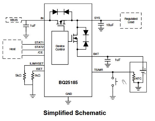
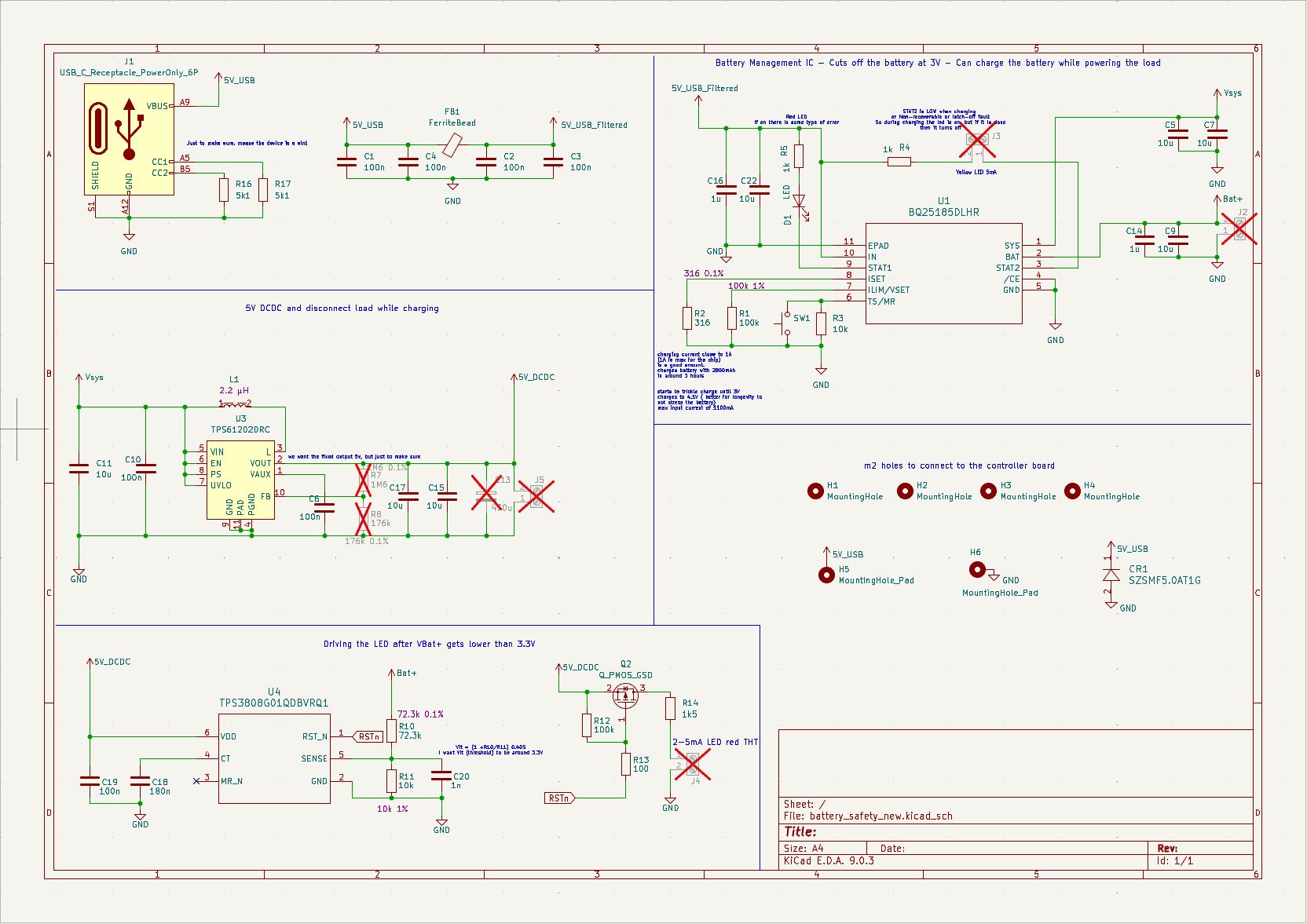

While charging through the USB-C port, the current runs through a PI-Filter, through the BQ25185DLHR to the battery to charge it and supply the load at the same time like indicated in figure 5. It is normally said to charge up to 4.2V, but again to ensure the longevity of the battery I decided to charge up to 4.1V. This can be set at the Ilim port on the BQ25185DLHR. I´ve used a 100kOhm (figure 4) resistor to set the current limit at 1.1A and the voltage limit at 4.1V (table 8-1 in datasheet). On the ISET-pin the fast-charge-current is set through the formula
I_CHG = K_ISET/R_ISET = 300 AOhm / 316 Ohm = 0.95A
I wanted to stay a little below the maximum of 1A, just to be safe. Since the batteries have a capacity of 2850 mAh, the charging takes 2-3 hours. To indicate the charging, I will connect a Yellow LED which will be seen on the housing later on. The LED turns of when the charging is done. Below around 3.3V the comparator will turn on red LED to indicate low battery voltage. Of course this will then draw an extra current of around 3-5 mA. This is not a problem since it is intended to warn the user to charge the device. As mentioned before, the battery disconnects completely when falling below 3V. When the load disconnects from the battery, the voltage usually rises a bit. This would connect the load to the battery again. However for that reason there is the VBUVLO_HYS of around 150 mV which means that it will only connect the load again after it rises up to 3.15 V. These characteristics are all built-into the chip. Many applications have a separate IC for the safety and turn-on/turn-off mechanisms.
First Annoying Problems
After designing and ordering the board, I tested it out. So I connected it to the LoRa devices. I faced 2 problems at once. Both the sender and receiver were discharged after around 5 days. Since the sender should draw a smaller current than the receiver, because it is usually in DORMANT mode, I suspected a "leak" or abnormal current loss on the way. If the battery is at 2800 mAh and it takes around 5 days * 24 hours to be empty the "SLEEP" current is around 20 mA, maybe higher maybe lower, but either way it´s way too high.
Looking at the sender device, the PI Pico should should turn off the E-Ink display before going into DORMANT, and the datasheet of the PICO states (datasheet page 15) a current lower than 1 mA. The first thing I have done, was trying to measure the current which goes out to the LoRa-board through the terminal block "5V Load" on the bottom of figure 6.

After trying it out with my amp-meter, I remembered that it is an extremely cheap one, which cannot measure lower currents accurately. Then I thought thought of cutting the plane open which connects the "Battery"-terminal block to the BQ25185DLHR. This would show me the drawn current from the battery. That cut can be seen on figure 6 as well (arrow going to the highest place). I wanted to place a 10 Ohm resistor in between, but this made it way worse, it started chirping and ringing and didn´t work anymore. The voltage drop on the resistor probably got too big, meaning the boost converter pulled a current that made the Charging-IC turn off and on. That is probably what the problem was, so I replaced it with a 1 Ohm resistor and some extra caps to just to make sure. Still, it didn´t work, which makes kind of sense, beacause the boost converter frequency might have created voltage spikes and a drop big enough to make the BQ go into UVLO. It worked with a simple resistor instead of the LoRa-board though, but that wasn´t my solution.
I decided to build a simple current monitor with these INA226 boards(see other project), to not have a big impact on the measured circuit and also get pretty valid current values. The shunt there is .1 Ohm and with my configuration can measure up to 800 mA. I connected it in between the Charging-IC and boost converter and it displayed a current of around 20 mA as estimated. Then I connected it between "5V Load" and the LoRa device and it showed around 9 mA. The comparator in "OFF mode" doesn´t draw a significant current, so the DCDC itself wasted around 10mA, but also the LoRa device was not as expected.
"Power-Safe-Mode"
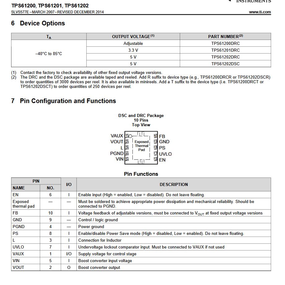
I did look at the datasheet beforehand, but didn´t waste a second thought on the PS pin (figure 7) of the TPS61202DRC I thought "yeah it´s probably to make it even less power consuming" and connected the PS-pin to VIN like in the examples in the datasheet. After desoldering the IC and cutting open the connection, it really changed to below 1 mA when no load is connected, while it was 10mA before.
Think twice before buying cheap amazon board copies!
In most cases, if you buy the RP2040 on Amazon they will work exactly like the original boards. One of the few excetions is the DORMANT mode. The DORMANT mode is normally the lowest power mode, because everything even the clocks and PLL´s stop. To make it short, because of the low cost parts on this board the DORMANT mode currents vary from 2 mA(only one of 4 boards was 2 mA) to 6 mA on the Amazon boards. After ordering the original board from berrybase and using the same code, the dormant current was suddenly as low as stated in the datasheet. One board drained 0.7 mA and the other one 0.9 mA. After being satisfied with that, I needed to fix another problem but only could do that for the sender device. I have tried to put the LoRa devices to sleep before putting the sender into DORMANT and receiver into rtc sleep mode. It didn´t work for the receiver, but I thought that 2 mA are not that bad. Since I wanted to get rid of that as well, I now tried it again. On the sender it works, but the receiver doesn´t work. I don´t know if it has to do with the LoRa library, but I have tried reinitializing SPI and resetting the device with every rtc wake up. It didn´t work. However, I didn´t want to waste more time on that, because that meant to go through the whole firmware, which I didn´t want to do.
Now the whole sender board draws around 0.9 mA in DORMANT mode and the receiver board around 6-9 mA. This is an extreme difference and should ideally be equal. If the receiver was in DORMANT as well it would be fixed. This can be done with a low power lora device that wakes up on a "sensed" signal, but we have to accept it like it is at this point.
Lastly, I decided to remove the Boost Converter after realizing that all my devices can run with 3.3 V and there is a Buck-Boost-Converter on the PICO. The amount of current which is drawn during their "communication-time", can be handled by the on-board dcdc. Instead I soldered a schottky diode onto the board to prevent currents flowing back to the Charging-IC(figure 8).

The chirping from before...
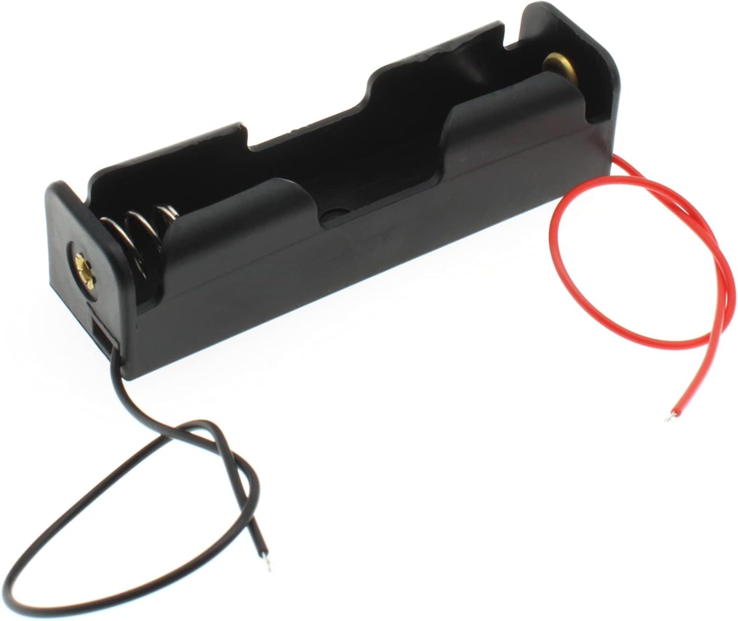
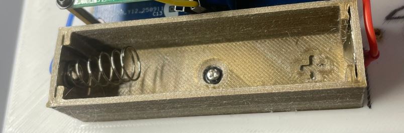
So the chirping of the Charging-IC that appeared when I wanted to solder a 1 Ohm resistor into the VIN plane, didn´t actually only appear there. As indicated before it starts chirping and ringing when the impedance before the boost converter is "too high". At least I think that´s what it is. After a while, I found out that the battery holder (figure 9) also produces the chirping(I think the impedance was too high, because of the poor crimping). I wanted to 3d-print a new holder, with better battery spring plates and therefore a lower impedance. You can see in figure 10 the custom holder, that actually eliminated the problem.
Conclusion
To conclude the paragraph on the problems with this board, we now have significantly reduced the power loss of the boost converter and the chirping because of the battery holder. Additionally, we realized that only the original pico go into a low power sleep mode, so the problem were the Amazon ones. The output of the board now supplies battery voltage - shottky voltage to the Buck-Boost-Converter of the pico which then powers the pico itself, LoRa device and E-Ink display. I wouldn´t recommend powering devices through the pico, if there were bigger loads though. On the other hand, we now have a charging board, which allows the usage of the device, while charging, also an indicaion for low battery voltage. The next step is printing a housing and finally to put it all together and test it.